Solar Wafer Manufacturing
Solar wafer manufacturing is a crucial stage in the production of photovoltaic (PV) cells, the core components of solar panels. These wafers, typically made from high-purity silicon, serve as the foundation for converting sunlight into electrical energy through the photovoltaic effect. The process of solar wafer manufacturing involves advanced technologies and precision techniques to ensure the production of high-quality wafers essential for efficient solar power generation.
Key Steps in Solar Wafer Manufacturing:
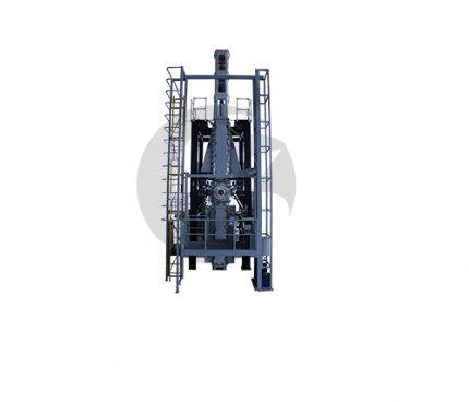
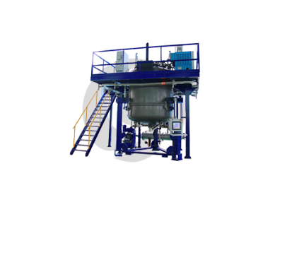
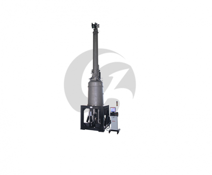
- Silicon Ingot Production: The process begins with the production of silicon ingots, which are large cylindrical blocks of high-purity silicon. This is typically achieved through the Czochralski process or the float-zone method, both of which involve melting and crystallizing silicon in a controlled environment to produce single-crystal ingots.
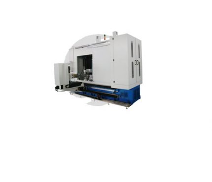
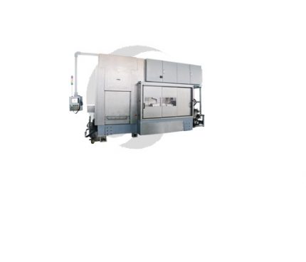
- Wafer Slicing: Once the silicon ingots are formed, they undergo wafer slicing to produce thin, circular discs known as wafers. Diamond saws or wire saws are used to precisely cut the ingots into wafer slices with uniform thicknesses, typically ranging from 150 to 300 micrometers.
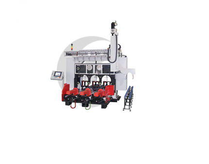
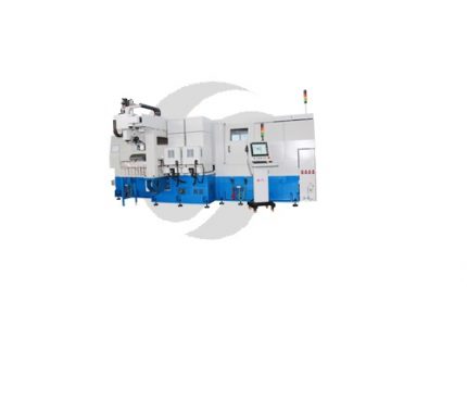
- Surface Treatment: After slicing, the wafer surfaces undergo various treatments to remove defects, impurities, and surface roughness. This may involve processes such as lapping, etching, and polishing to achieve the desired surface quality and smoothness.
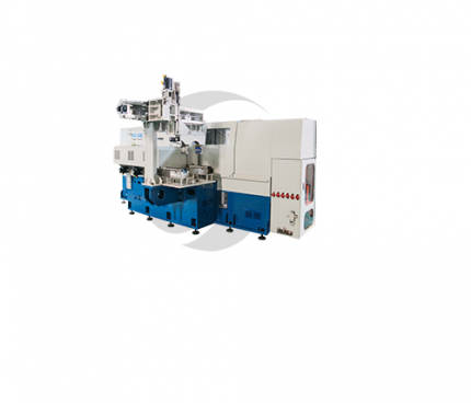
- Doping: Doping is the process of introducing impurities, such as phosphorus or boron, into the silicon wafer to modify its electrical properties and create the necessary p-n junctions for photovoltaic operation. Doping is typically achieved through diffusion or ion implantation techniques.
- Texturing: To enhance light absorption and reduce reflection losses, the surface of the silicon wafer is textured using chemical etching or mechanical processes. Texturing creates a rough surface morphology that traps incoming sunlight, increasing the chances of photon absorption within the wafer.
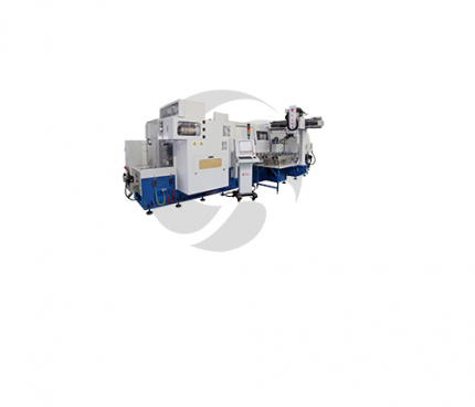
- Cleaning and Inspection: Throughout the manufacturing process, wafers undergo rigorous cleaning and inspection procedures to ensure they meet quality standards. Cleaning removes contaminants and residues that may affect wafer performance, while inspection verifies dimensional accuracy, electrical properties, and surface quality.
Technological Advancements and Innovations:
Solar wafer manufacturing has seen significant advancements and innovations aimed at improving efficiency, reducing costs, and enhancing performance. Key innovations include:
- Thin Wafer Technologies: Advanced wafer slicing techniques and material innovations have enabled the production of thinner wafers, reducing material consumption and increasing cell efficiency.
- Kerfless Wafer Production: Kerfless wafer production methods, such as epitaxial growth and layer transfer techniques, minimize material wastage by eliminating the need for sawing, resulting in higher yields and lower costs.
- Kerf Recovery: Techniques for recovering and recycling silicon kerf, the material lost during wafer slicing, have been developed to further improve resource efficiency and reduce environmental impact.
- Monocrystalline and Multicrystalline Wafers: Advances in crystalline silicon technology have led to the development of high-quality monocrystalline and multicrystalline wafers with improved efficiency and performance characteristics.